Introducing EXAM: NEXony's Cutting-Edge Inspection Platform
EXAM is NEXony’s advanced inspection platform, designed to meet the complex needs of the semiconductor industry and similar applications. By combining high-end components, modern software, and innovative thinking, EXAM delivers outstanding performance and unparalleled results.
Learn more about the features, benefits, and capabilities of EXAM in the following sections, and discover how this versatile platform can transform your inspection processes.
EXAM is NEXony’s advanced inspection platform, designed to meet the complex needs of the semiconductor industry and similar applications. Learn more about the features, benefits, and capabilities of EXAM in the following sections.
Module "A"
Module "S"
Module "E"
Module "A"
Module "S"
Module "E"
A ... the area advantage
Dive down...
Stay focussed...
Top down
More than RGB
...and more!
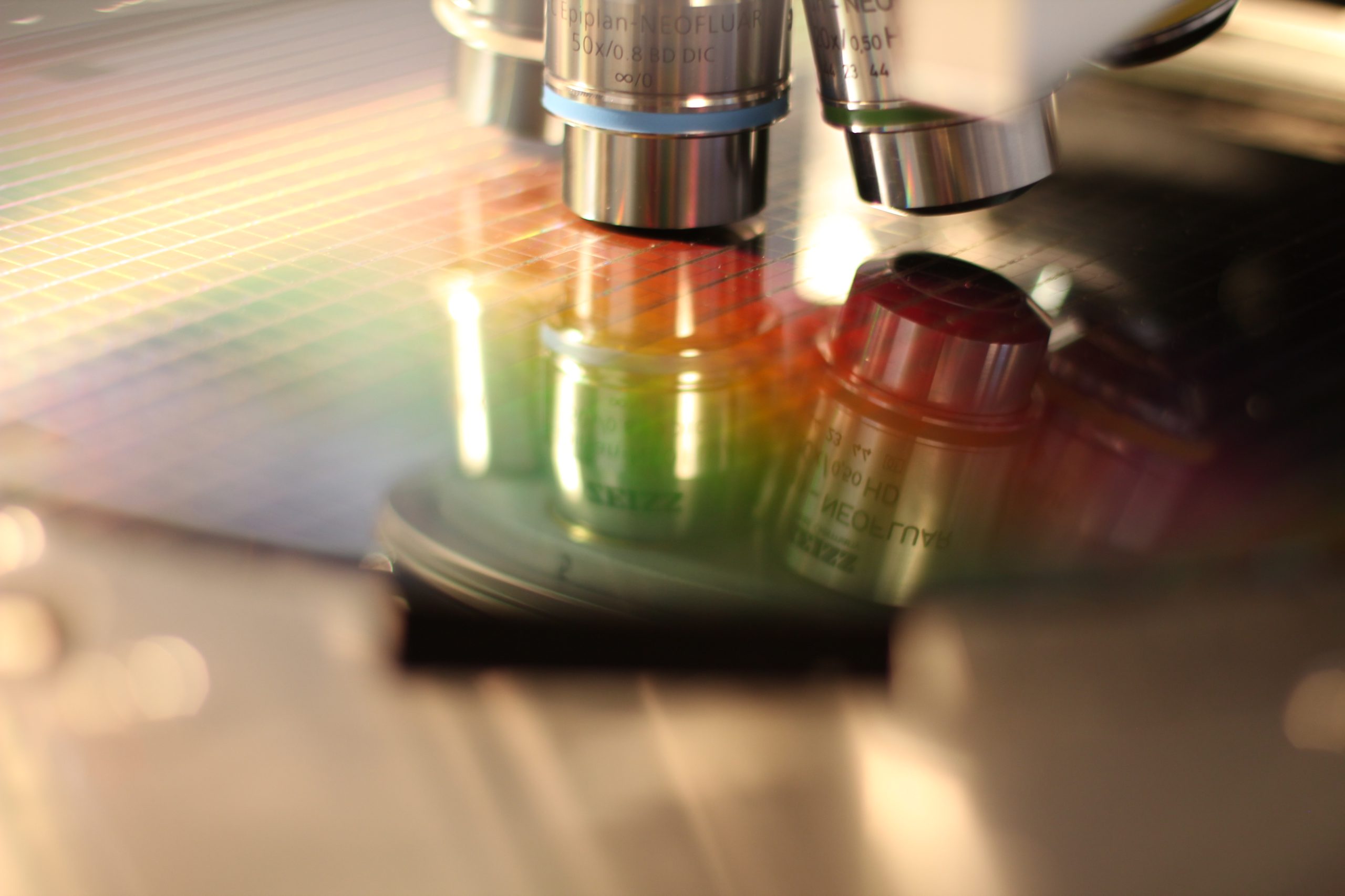
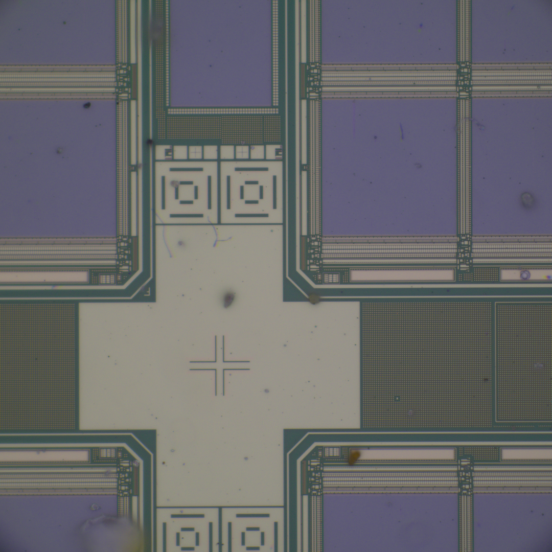
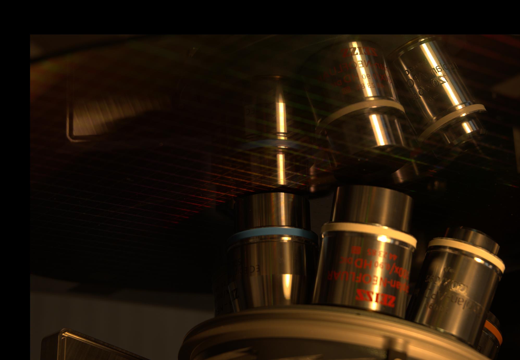
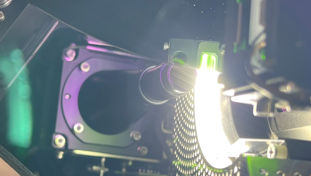
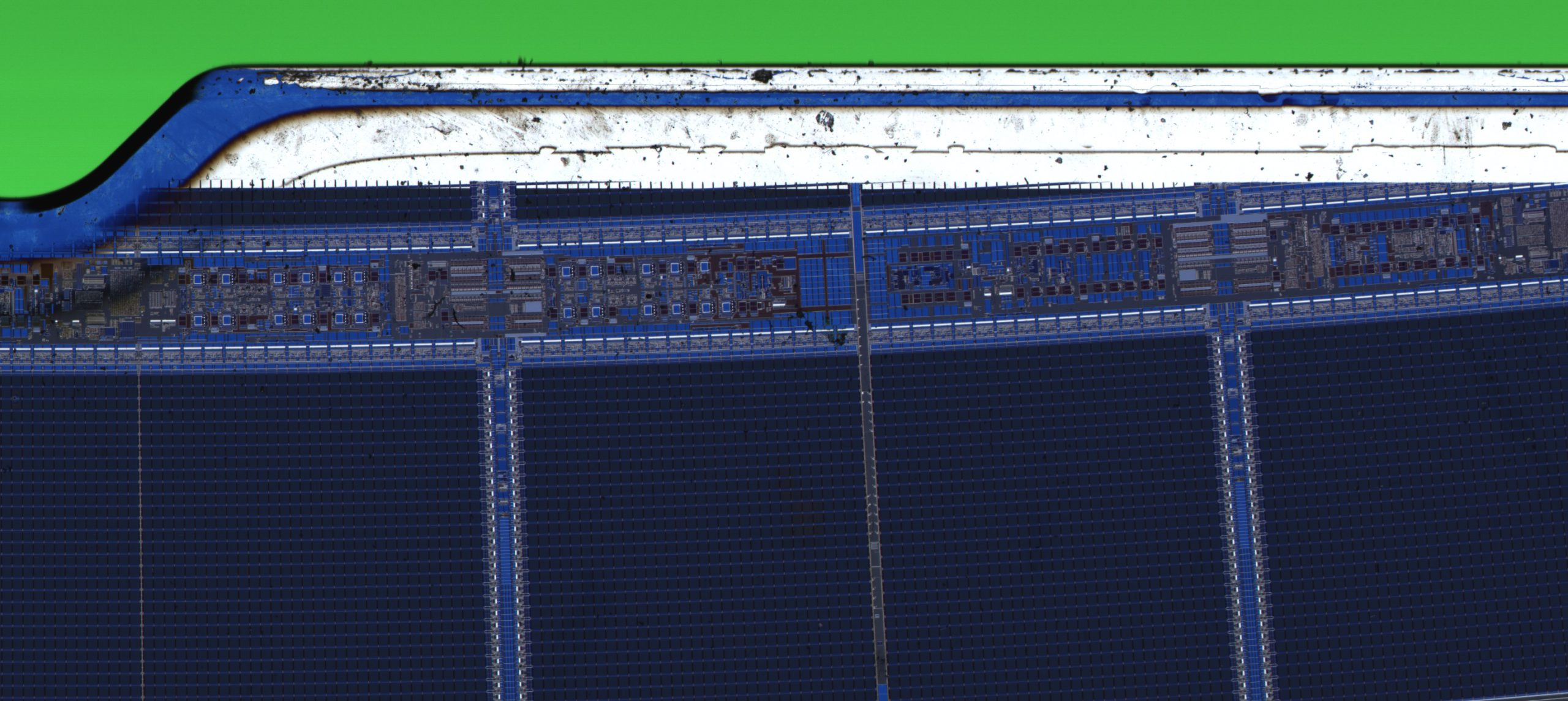
Our state-of-the-art microscope is designed to deliver the best possible results. Equipped with up to 7 ZEISS lenses it offers exceptional optical quality and versatility for a wide range of microscopic applications.
Advanced Illumination Setups that provides optimal lighting conditions for various sample types and analysis requirements in combination with High-Speed Color Imaging System Enabling fast and accurate image capture with exceptional color fidelity.
Customizable Optical Setup
The microscope’s optical setup can be tailored to specific needs with additional elements, such as
Motorized Diaphragms: Allowing for precise control over illumination and image quality.
Filters: Enabling the selection of specific wavelengths or polarization states for enhanced image contrast and analysis.
…with Advanced Autofocus Technology!
Our microscope optics feature a cutting-edge laser autofocus module, designed to ensure precise focus control and optimal image quality. Key features include:
Segmented Line Projection: A state-of-the-art laser system projects a segmented line into the image, accurately determining the best focus level.
Dual Autofocus Approach: In addition to laser autofocus, an image-based autofocus mechanism (video autofocus) is implemented to handle challenging structures and ensure reliable focus control.
Unwavering Focus for Exceptional Results
With our advanced autofocus technology, you can rely on precise focus control, even in complex imaging applications, to achieve exceptional results and accurate data.
EXAM-A offers advanced inspection capabilities, enabling simultaneous inspection of the wafer’s front and backside. For applications requiring detailed backside inspection, a microscope system with comparable capabilities to the frontside system can be installed, ensuring comprehensive wafer analysis. Inspect both sides of the wafer with high precision and accuracy.
Flexible Configuration: Tailor the system to meet specific inspection requirements, whether frontside, backside, or simultaneous inspection is needed.
With EXAM-A’s dual-side inspection capability, you can achieve thorough wafer analysis and ensure the highest quality standards in your production process.
Enhanced Wafer Analysis with Hyperspectral Capabilities
The optional hyperspectral imaging module offers a powerful tool for monitoring the full wafer surface in parallel with microscopic applications. This advanced capability enables:
Film Thickness Deviation Detection: Identify variations in film thickness and other issues that affect spectral responses.
Comprehensive Surface Analysis: Monitor the entire wafer surface, providing valuable insights into material properties and potential defects.
By integrating hyperspectral imaging into your wafer analysis workflow, you can gain a deeper understanding of your materials and processes, enabling more effective quality control and process optimization.
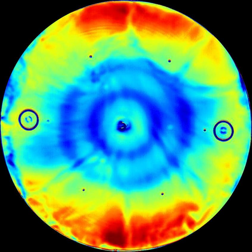
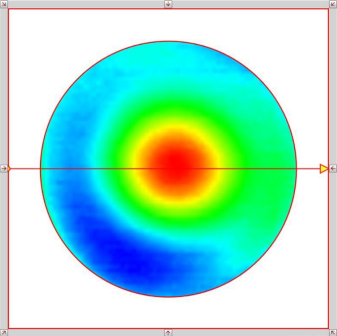
Example: Contactless wafer resistivity measurement
The “A” module was designed with a primary focus on microscopic applications, but its architecture also allows for seamless integration of additional technologies and sensors. This flexibility enables the module to
Address Specific Needs: Adapt to unique requirements and applications, ensuring the module remains relevant and effective.
Future-Proof Your Investment: Easily incorporate new technologies and sensors as they become available, extending the module’s capabilities and lifespan.
The contactless wafer surface resistivity measurement option is just one example of platform option. Get in contact with us to learn more about it.
A ... the area advantage
Dive down...
Stay focussed...
Top down
More than RGB
...and more!
Our state-of-the-art microscope is designed to deliver the best possible results Equipped with up to 7 ZEISS lenses it offers exceptional optical quality and versatility for a wide range of microscopic applications.
…with Advanced Autofocus Technology!
Our microscope optics feature a cutting-edge laser autofocus module, designed to ensure precise focus control and optimal image quality.
EXAM-A offers advanced inspection capabilities, enabling simultaneous inspection of the wafer’s front and backside. Inspect both sides of the wafer with high precision and accuracy.
The optional hyperspectral imaging module offers a powerful tool for monitoring the full wafer surface in parallel with microscopic applications. This advanced capability enables Film Thickness Deviation Detection and Comprehensive Surface Analysis.
The contactless wafer surface resitivity measurment option is just one example of platform option. Get in contact with us to learn more about it.
S ... like Snapshot !
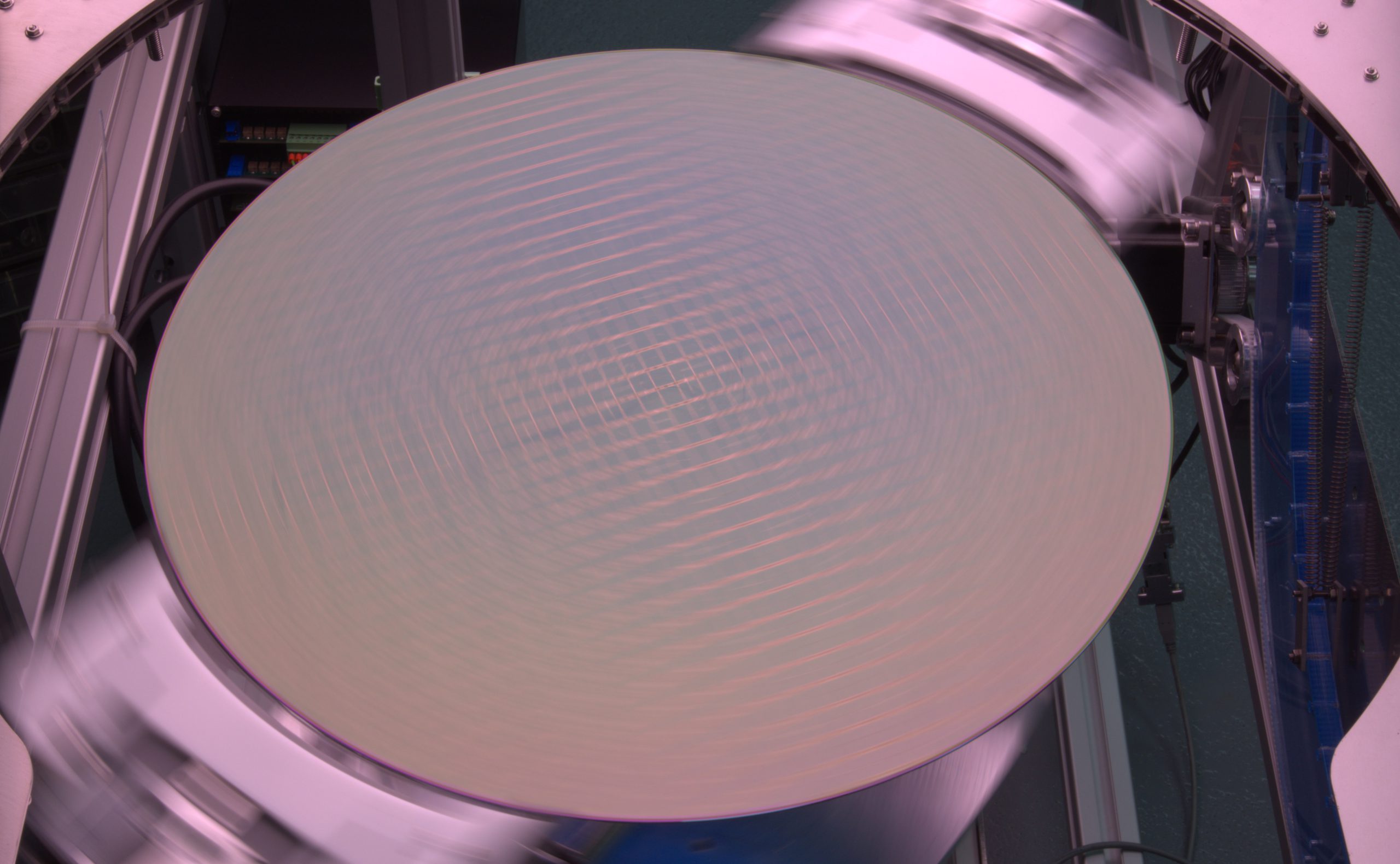
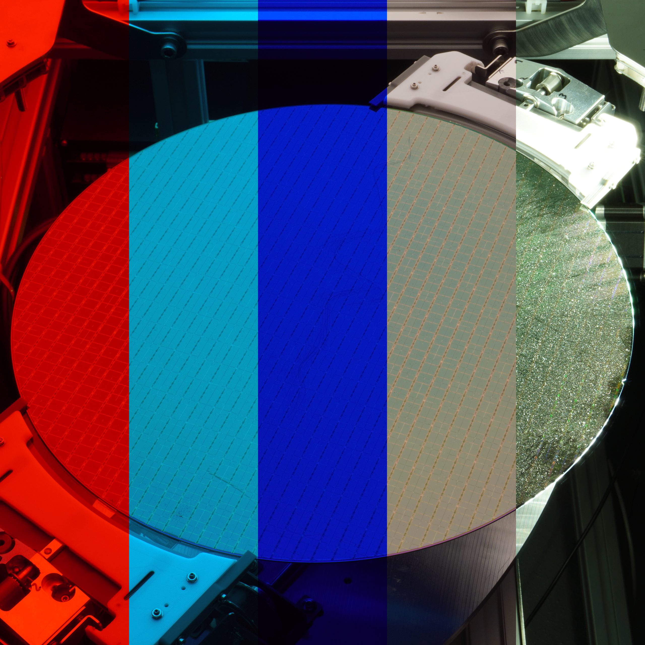
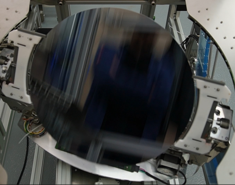
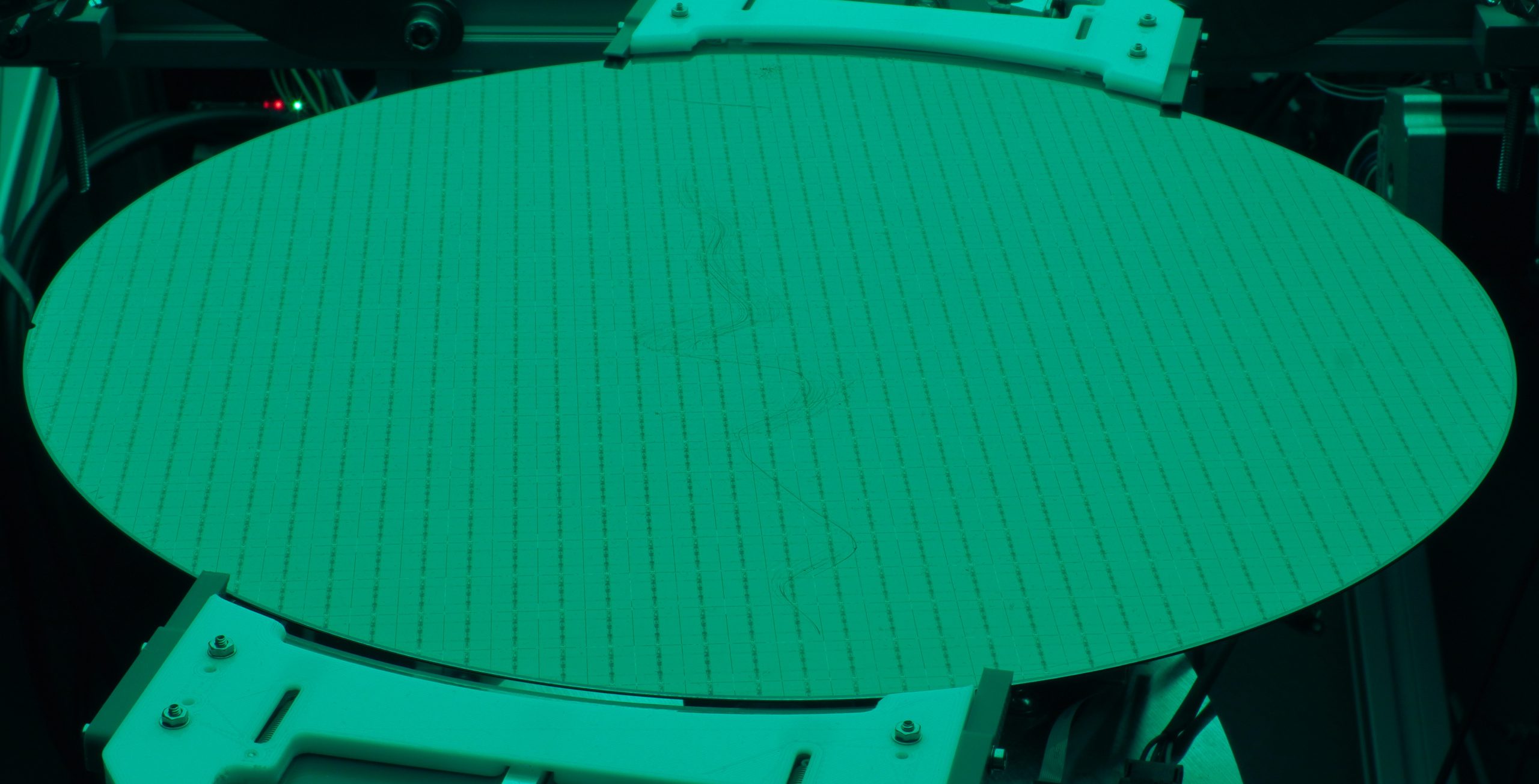
Full wafer...
Different perspectives...
Turn on the light...
Fast and simple...
Automate the detection...
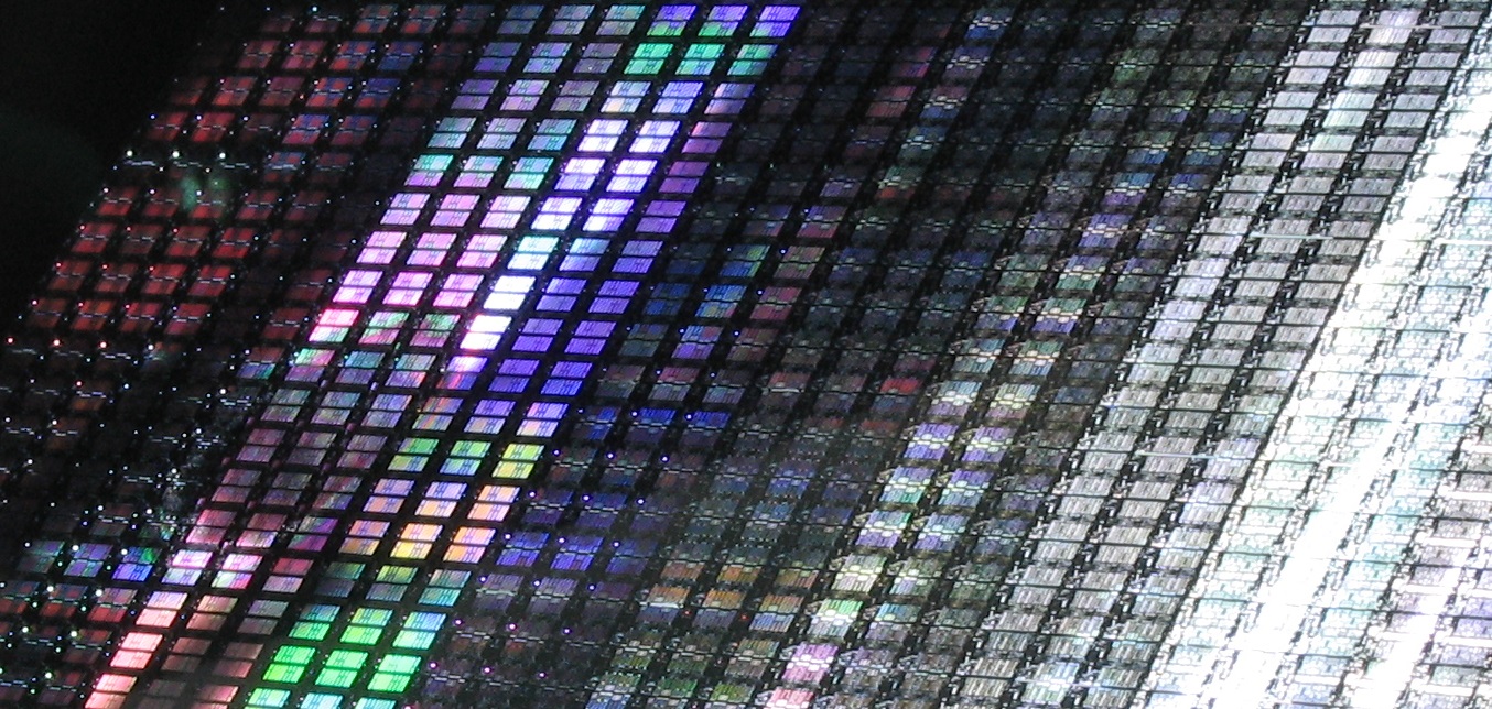
…images from frontside and backside – this is what it is made for. The wafer gets gripped at the outer edge and just a minimum of edge and surface gets covered. Within a few seconds, both wafer front- and backside can be captured by a digital camera system.
…are realized by the wafer tilt- and rotation mechanics. Depending on the defect type that gets hunted, the system can provide multiple images from different viewpoints to ensure the best environment for a safe detection.
…and see! EXAM_S is equipped with several light sources. For brightfield imaging, an RGB-illumination can be used to make the interesting things visible. Additional high- power darkfield illumination helps to make tiny particles and scratches visible.
… – the approach of Snapshot. With a throughput of up to 200wph, the module offers a high speed prodution control mechanism. Integrated features for an automated notch detection helps make the module attractive as a cost-effective standalone solution.
…with the help of deep learning capabilities. Snapshot is prepared to get trained on real images by operators with experience. Once enough training data were fed, the tool can operate with the generated DL models and helps to detect anomalies automatically.
S ... like Snapshot !


Full wafer...
Different perspectives...
Turn on the light...
Fast and simple...
Automate the detection...
…images from frontside and backside – this is what it is made for. The wafer gets gripped at the outer edge and just a minimum of edge and surface gets covered – front- and backside!
…are realized by the wafer tilt- and rotation mechanics. Depending on the defect type that gets hunted, the system can provide multiple images from different viewpoints to ensure the best detection.
…and see! EXAM_S is equipped with several light sources. For brightfield imaging, an RGB-illumination can be used. Additional high- power darkfield illumination makes tiny particles and scratches visible.
… – the approach of Snapshot. With a throughput of up to 200wph, the module offers a high speed prodution control mechanism. Integrated features for an automated notch detection helps make the module attractive as a cost-effective standalone solution.
…with the help of deep learning capabilities. Snapshot is prepared to get trained on real images by operators with experience. Once enough training data were fed, the tool can operate with the generated DL models and helps to detect anomalies automatically.
E ... like Edge !
Nothing remains hidden
Fast and accurate
Multiple wafer sizes
Hit at apex
And more...
EXAM_E provides a seamless imaging system to cover the full wafer edge without missing something. Based on multiple cameras, the wafer edge is grabbed from all sides simultaneously.
Under standard condition a wafer scan tooks less then 8s. For more challenging tasks, additional capabilities like stacked imaging, extended exposure and transparent substrate support is already on board.
The module is prepared to run multiple wafer sizes as an optional extension. There is no need to modify any hardware to switch the system, e.g., between 200 and 300mm or 150 and 200mm wafers.
The E(dge) module offers high resolution images from all perspectives. Problems caused by residuals of wafer edge damages located on the wafer apex zone are not longer invisible.
The detection capablilities can be combined with simple metrology tasks like edge bead removal measurements.

